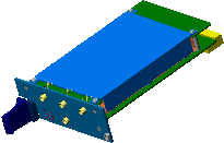
Electronics Packaging

  • Schematic entry, hierarchically arrangement for maximum flexibility, logical and understandable. Most popular electronic input and output formats supported. Tightly coupled to the pwb design for maximum control of placement, line widths, and design rules.

  • Printed wiring board layout, RF, digital, power, analog, or special applications such as membrane switches and panel graphics. Most popular electronic input and output formats supported. Fast turn prototyping to fully documented production. Extensive design rule control and reporting capabilities.

  • Electro-mechanical module design, in any form factor. Complete module design from pwb design to front panel graphics or any portion thereof. Unique shielding solutions allow mixed technology, high density packages.

  • Innovative solutions to your complex packaging problems. Innovation needn't be expensive. We'll use common tools and technology in new and unique ways to solve your design issues.

  • Special projects, burn in fixtures, device package adaptors, potted module design, RF shielding, etching masks etc.

JMC Design Services

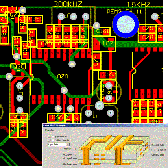
JMC Design Services offers the complete solution to your electronic packaging needs. Schematic entry, PWB layout, module design, or full system configuration, JMC Design Services has the tools and expertise to assist with any phase of your product's development or to be your turn-key solution to design success.

© 2006 John M. Cardone. All rights reserved

Phone: 530.436.2216

Cell: 805.796.0787

Web address: http://www.jmcdesignservices.com

Email:   jmc@jmcdesignservices.com

JMC Design Services

P. O. Box 397

Grenada, CA. 96038-0397